

Bead Mill for CMP Slurry Dispersion: Where a Single Oversized Particle Can Ruin a Wafer

Author: Moeez Ullah Published: September 11, 2026
Bead Mill for CMP Slurry Dispersion: Where a Single Oversized Particle Can Ruin a Wafer
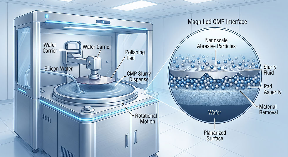
CMP (chemical mechanical planarization) slurry uses nanoscale abrasive particles — typically colloidal silica or ceria — suspended in a chemical solution to polish semiconductor wafers to atomic-level flatness.
Unlike most dispersion applications, a small number of oversized particles in CMP slurry can cause measurable wafer scratch defects, even when the average particle size looks acceptable.
Published formulations commonly specify silica and ceria particle sizes in the 4–120nm range, with some slurries deliberately combining two abrasive types at different concentrations to balance removal rate and selectivity.
Particle size directly affects both removal rate and material selectivity — the ability to polish one film material faster than another in the same process step.
As semiconductor manufacturing pushes toward more advanced nodes and more complex multi-material stacks, CMP slurry particle size control becomes a more consequential yield factor, not a smaller one.
At a Glance | Detail |
Focus keyword | Bead mill for CMP slurry dispersion |
Core materials | Colloidal silica, ceria (cerium oxide), sometimes alumina |
Why this is unique | A tiny fraction of oversized particles can cause scratch defects that ruin an entire wafer |
Typical particle size range | Roughly 4–120nm, depending on abrasive type and target film |
Key process metrics | Removal rate, selectivity (film-to-film), defect/scratch density |
Why it matters now | Advanced semiconductor nodes and multi-material stacks demand tighter slurry control |
What is CMP slurry? Chemical mechanical planarization (CMP) slurry is a nanoscale abrasive dispersion — commonly colloidal silica or ceria particles suspended in an acidic or basic chemical solution — used to polish semiconductor wafers flat during chip manufacturing. Why does dispersion quality matter so much here? Because a bead mill for CMP slurry dispersion isn't just controlling average particle size — it's controlling the presence or absence of the rare oversized particles that can physically scratch a wafer and turn a multi-thousand-dollar chip into scrap.
Why CMP Slurry Breaks the "Average Particle Size" Rule

The Defect Risk Isn't About the Average — It's About the Outliers
Does the average particle size tell you everything you need to know about a CMP slurry? No. Technical guidance on CMP slurry process control is explicit that the abrasive particles' size distribution directly affects critical metrics including removal rate and wafer defects — and that detecting and controlling remaining large particles is a distinct, ongoing process control requirement, separate from managing the mean particle size (CMP slurry process control overview, HORIBA). A slurry with an excellent average particle size can still cause defects if even a small population of oversized particles or agglomerates is present.
Why Spherical, Uniform Particles Matter Beyond Just Size
Colloidal silica is widely favored in CMP applications specifically because of its clean, spherical shape produced by the sol-gel synthesis method, which causes measurably less polishing damage than irregularly shaped abrasive particles of the same nominal size. Shape uniformity, not just size, is part of what determines whether a given abrasive particle scratches or smoothly polishes the wafer surface it contacts.
How Particle Size Directly Controls Removal Rate and Selectivity

Smaller Particle Size, Different Removal Behavior
Does particle size affect how fast CMP slurry polishes different materials? Yes, directly and measurably. Patent formulation data has shown that varying silica particle size from 30nm to 120nm and ceria particle size from 30nm to 80nm produced measurably different polishing selectivity results between organic and TEOS oxide layers in controlled testing, with one formulation reporting a selectivity ratio above 23.9 when using a 120nm-or-smaller silica particle size (CMP slurry composition and selectivity study, patent US9343326). That's a direct, quantified link between a dispersion parameter and a process outcome semiconductor manufacturers depend on.
Two Abrasives Can Work Better Together Than Either Alone
Can combining abrasive particle types improve CMP performance? In some formulations, yes — patent data on tantalum nitride and silicon dioxide polishing found that silica particles alone or ceria particles alone each produced an impractically low polishing rate for certain films, while a dispersion combining both particle types at specific concentrations achieved a practical, usable polishing rate that neither abrasive delivered independently (CMP slurry dual-abrasive formulation patent, US6896590). Getting that kind of multi-abrasive dispersion right depends on both particle types being uniformly and stably dispersed relative to each other, not just individually well-ground.
The Processing Challenge: Precision Without Introducing Contamination
Why Copper and Advanced-Node CMP Slurries Push Particle Size Even Finer
Patent formulation work on copper CMP slurries has tested precipitated and fumed silica abrasives with mean particle sizes ranging as fine as 4nm up to roughly 700nm, identifying optimal formulations using precipitated silica under about 100nm for specific polishing performance targets (copper CMP polishing slurry patent, US7427567). As advanced semiconductor nodes shrink further, the tolerance for oversized particles or agglomerates in these formulations only gets tighter.
Why Agglomeration Control Matters as Much as Initial Particle Size
Because even a small fraction of agglomerated or coarse particles can cause scratch defects, CMP slurry dispersion has to prevent agglomeration through the full production and storage lifecycle — not just at the point of initial grinding — which places real weight on dispersant chemistry and process stability working together with the milling step itself, a pattern seen across several precision dispersion applications covered elsewhere in this series.
How Sanxing's Bead Mill Technology Supports CMP Slurry Production
Precision Particle Size and Distribution Control
Because CMP slurry quality depends as much on eliminating the oversized-particle tail of the distribution as on hitting a target average, Sanxing's vertical bead mill platforms — with adjustable rotor speed, bead loading, and circulation grinding — support the kind of controlled, repeatable dispersion process needed to narrow that distribution consistently, batch after batch.
Contamination Control for High-Purity Applications
Given how sensitive semiconductor manufacturing is to contamination of any kind, wear-resistant, chemically compatible wetted components in the grinding chamber matter as much for this application as they do for the pharmaceutical and battery-material applications covered elsewhere in this series.
Lab-Scale Validation Before Production Commitment
Because CMP slurry formulations are highly specific to the target film material and process node, validating a specific abrasive type, particle size target, and dispersant system at lab scale on Sanxing's F4/W Series bead mills before committing to production batches reduces the risk of costly reformulation after defect testing reveals a problem.
CMP Slurry Dispersion vs. General Pigment/Abrasive Dispersion

Factor | General Pigment/Abrasive Dispersion | CMP Slurry Dispersion |
Primary quality metric | Average particle size and color/strength properties | Elimination of oversized-particle outliers, not just average size |
Consequence of a rare large particle | Minor defect or inconsistency | Wafer scratch, potential total yield loss on that unit |
Shape sensitivity | Generally low | High — spherical particles cause measurably less polishing damage |
Multi-material formulation complexity | Moderate | High — dual-abrasive systems tuned for selectivity between films |
Contamination tolerance | Application-dependent | Extremely low — semiconductor-grade purity required |
Why This Market Is Worth Targeting Now
Semiconductor manufacturing continues pushing toward more advanced process nodes and increasingly complex multi-material film stacks, both of which raise the bar on CMP slurry precision — tighter particle size distributions, more sophisticated selectivity control between film materials, and lower tolerance for defect-causing outliers. As that precision requirement climbs, the dispersion equipment and process control behind CMP slurry production becomes a more direct factor in semiconductor manufacturing yield, not a peripheral formulation detail.

Conclusion
CMP slurry dispersion carries some of the tightest tolerances in this entire series — not because the average particle size target is unusually extreme, but because the cost of a single overlooked outlier particle is a scrapped semiconductor wafer. Contact Sanxing Feirong Machinery to discuss bead mill configuration for CMP slurry and precision abrasive dispersion applications.
Frequently Asked Questions
Why is CMP slurry dispersion different from typical pigment or coating dispersion?
Because a small population of oversized particles or agglomerates — not just the average particle size can cause scratch defects on a semiconductor wafer, making distribution control and outlier elimination as important as hitting a target mean particle size.
Does particle size affect which materials a CMP slurry polishes fastest?
Yes, formulation studies have shown that varying silica and ceria particle size measurably changes polishing selectivity between different film materials, such as organic layers versus oxide layers.
Why do some CMP slurries combine two different abrasive particle types?
Because certain film materials don't polish at a practical rate with either abrasive type alone, while a combined formulation at the right particle sizes and concentrations achieves a usable polishing rate neither delivers independently.
Why does particle shape matter for CMP slurry, not just size?
Spherical, uniform particles (such as sol-gel-produced colloidal silica) are associated with measurably less polishing damage than irregularly shaped particles of similar size, since shape affects how the abrasive contacts and interacts with the wafer surface.
External Resources
https://www.horiba.com/int/materials/material-types/raw-materials-for-semiconductors/cmp-slurry/
https://image-ppubs.uspto.gov/dirsearch-public/print/downloadPdf/9343326
https://image-ppubs.uspto.gov/dirsearch-public/print/downloadPdf/6896590
https://image-ppubs.uspto.gov/dirsearch-public/print/downloadPdf/7427567


Comments